Dislocations
Defects of the crystal lattice
Dislocations are linear defects inside a crystal lattice and govern the plastic behaviour of a material. Since dislocations cannot end somewhere inside a crystal, they must either form dislocation loops or reach the surface. That is where we can see them by STM.
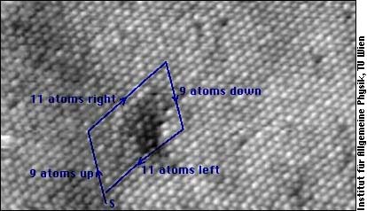
A dislocation is characterized by its Burgers vector: If you imagine going around the dislocation line, and exactly going back as many atoms in each direction as you have gone forward, you will not come back to the same atom where you have started. The Burgers vector points from start atom to the end atom of your journey (This “journey” is called Burgers circuit in dislocation theory):

Of course, one cannot see the dislocation line on an STM image, since it leads into the bulk, but only its end. Dislocations like the above one, where the Burgers vector is perpendicular to the dislocation line, are called edge dislocations.
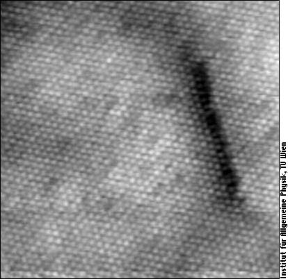
A dislocation may split into two partial dislocations, where the Burgers vector of each partial is less than one interatomic distance. Such partial dislocations span a stacking fault between them. At the surface, the stacking fault is often seen as a small step with a height of less than one atom layer. The lower side of this “1/3 step” looks dark in the following STM image.

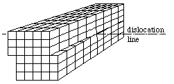
A dislocation with its Burgers vector parallel to the dislocation line is called screw dislocation:

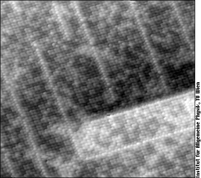
And that's what it looks like in an STM image: A step begins at the dislocation core.

One side-remark for dislocation experts: Strictly speaking, the Burgers vector is not exactly perpendicular to the surface here, but rather 45° inclined, whereas the dislocation line is roughly perpendicular to the surface (we can't see that, it follows from theory). Therefore, the dislocation has a screw and an edge component (mixed dislocation). Only the screw component is immediately obvious in the STM image, however.
The above image also shows a shifted row reconstruction (single rows of atoms brighter than the surrounding) and different apparent heights (grey levels) of the atoms in between due to carbon segregation. These phenomena are unrelated to the dislocation.
For further information
All STM images on this page show surfaces of PtNi alloys. On these surfaces, preferential sputtering leads to the formation of a Pt-enriched altered layer, which has a larger lattice constant than the underlying bulk. Therefore, misfit dislocations are created. Actually, the first two STM images of this page show such misfit dislocations. The screw dislocation shown is a defect of the bulk crystal.
- M. Schmid, A. Biedermann, H. Stadler and P. Varga
Lattice mismatch dislocations in a preferentially sputtered alloy studied by scanning tunneling microscopy
Phys. Rev. Lett. 69 (1992) pp. 925-928. Full text.
- M. Schmid, A. Biedermann, H. Stadler, C. Slama and P. Varga
Mismatch dislocations caused by preferential sputtering of a platinum-nickel alloy surface
Appl. Phys. A 55 (1992) pp. 468-475.
- M. Schmid, A. Biedermann, C. Slama, H. Stadler, P. Weigand and P. Varga
Preferential sputtering of Pt-Ni alloy single crystals studied by scanning tunneling microscopy
Nucl. Instrum. Meth. B 82 (1993) pp. 259-268.
If you want to become an expert in dislocation theory, a good textbook is
- J.P. Hirth and J. Lothe, Theory of Dislocations, second edition (Krieger Publishing, Malabar Florida 1982)
The one who reluctantly takes the responsibility for errors on this page:
Michael Schmid, IAP/TU Wien ([email address: lastname @ this server · enable javascript to see it]).