Electron Waves and Orbitals
Interference phenomena of surface and bulk states
As mentioned in the introduction to scanning tunneling microscopy, STM does not only show the geometric structure but it is strongly influenced by the electronic structure of the sample, i.e., the density of electronic states (DOS). Since electrons not always behave like particles but rather propagate as waves, we can see electron wave phenomena in STM images. These phenomena are very subtle, however, since the change of DOS is only a few percent, corresponding to apparent heights of a few pm (picometers). Compare this to the size of metal atoms, which are some 250 to 350 pm in diameter.
Surface states - waves
If there are electrons in a solid restricted to a region close to the surface (typically a few atomic layers deep), we call their states surface states. A good example for surface states can be observed on (111)-oriented Cu surfaces, where the wavelength of the surface state electrons at the Fermi energy (the energy probed by the STM in case of small sample voltage) equals approximately 14 interatomic distances. Since the STM is sensitive to the square of the wavefunction psi, we see both maxima and minima of the wavefunction psi as maxima of current or apparent height in the STM image, and, hence, the wavelength looks only half as long:
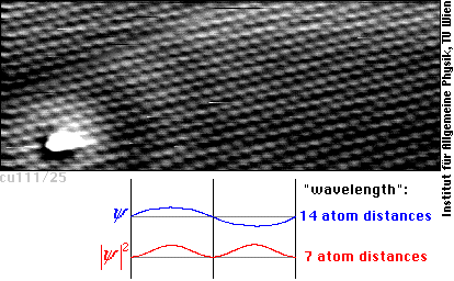
Only standing waves can be imaged by STM. In the above image a standing wave is created by scattering of the surface state electrons by at an impurity of unknown nature, which is probably situated above the surface (the white blob). Standing waves can also occur if the impurity atoms are located in the surface layer such as two substitutional Pb atoms in the following image, or even if the impurities are in deeper layers (as the impurity atoms responsible for the two rings in the top part of this image presumably are).
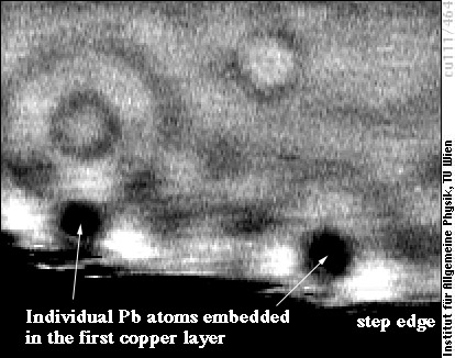
Image size is 10×8 nm (similar scale as the previous one, but no atomic resolution).
All these images were obtained at room temperature. At low temperatures the waves are much more pronounced (not smeared out by contributions of different energies), as shown in several great images obtained in Don Eiglers's group at IBM Almaden Research Center.
Surface states - orbitals
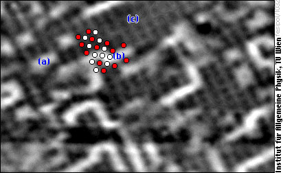
Surface states do not always look like waves, however. Have a look at the following STM image of a (100)-oriented surface consisting of nearly equal amounts of iron (some with white circles superimposed) and silicon atoms (red), created by Segregation of Impurity Atoms of Si out of bulk Fe. In most parts of the surface like the one marked ©, Fe and Si form a checkerboard-like structure of alternating Fe and Si called c(2×2) superstructure, with Si appearing dark in the STM image. There are also zigzag rows of Fe atoms (b), which form domain boundaries of the c(2×2) structure. (When you cross a domain boundary, Fe and Si atoms are exchanged with respect to their arrangement on the other side.) Finally, there are also small patches of pure Fe (a) not related to domain boundaries (one could also say, a few Si atoms replaced by Fe).
The striking feature of this image is the large brightness (high tunneling current) in regions (a) and (b) not covered by silicon. This is not a geometric effect, since it occurs only in a certain range of positive tunneling voltages. Hence, it must be rather due to the electronic structure of the surface. This is related to strong peaks in the tunneling spectra (the derivatives of the tunneling current vs. voltage curves, green lines):
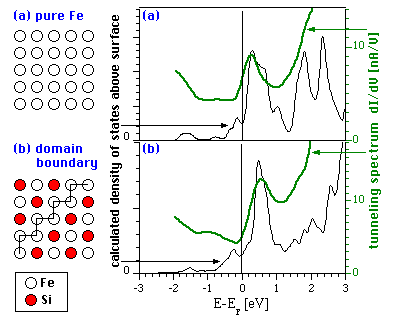
The solution to the puzzle can be found by calculations of the electronic structure of these surfaces: On pure Fe, a surface state reaching far into the vacuum (where the STM tip is probing the electronic structure) consisting of d-orbitals is found at just the energy observed in the tunneling spectra (+0.3 eV in spectrum (a), above). In domain boundaries of the c(2×2) structure shown above, the d-orbitals become tilted in such a way that the resulting density of the surface state reaching into the vacuum looks more like a band (and not like the zigzag row of the iron atoms), as you can see in the calculated density of states (white represents high density of the electronic state):
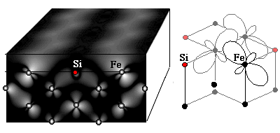
This not only explains the bright bands in the STM image above, but we also find good agreement with tunneling spectrum (b), showing that the peak is shifted to higher energies as the surface state is confined along the zigzag rows.
Of course, without the calculations, there is no way to see that the STM image actually shows tilted d-orbitals. The electronic structure inside the solid, which you see in this image, is not accessible to the STM tip.
Bulk states
On Aluminum surfaces (and probably on several other metals as well), a nice electron interference phenomenon can be observed: We create subsurface Argon bubbles by ion bombardment with Ar+ and subsequent annealing, which makes the implanted Ar atoms diffuse around and coagulate. Similar to the single impurity atoms in the examples above, these “large” objects can also scatter electrons, but in this case the “usual” electron states of the bulk electrons are affected.
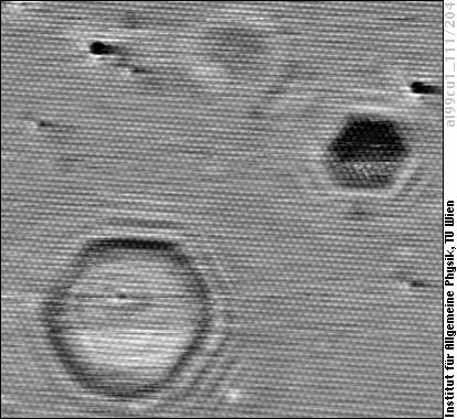
What we see in STM images of Al(111) looks like this:
The reason for the hexagonal shape of the interference patterns is the shape of the subsurface Ar bubbles, which minimize their surface energy. This leads to hexagonal (111) facets, as the Wulff construction for Al shows:

Since our surface is (111)-oriented, the top of each bubble is a small hexagon parallel to the surface, causing a hexagonal interference pattern. Scattering of electrons at the edges causes fringes, which are not waves propagating parallel to the surface as one might think looking at the STM image above. In a very simplified view, it rather looks like this:
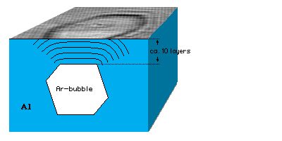
Since both the (outer) surface of the crystal and the top of the Ar bubbles are very efficient reflectors, standing waves of electrons form between them. Such an arrangement is called a quantum well. Unfortunately, we cannot directly look at a section through the sample to see the standing waves (the STM only probes the surface), but we can detect whether the electron wave fits nicely into the well or not. In the case of constructive interference (if the way back and forth is an integer number of wavelengths) we see an increase of tunneling probability, reflected by an increase of apparent height (the hexagon appears brighter than the surrounding). In the opposite case (destructive interference) the hexagon appears dark, as the one near the right edge in the image above. Whether constructive or destructive interference occurs depends both on the way the electron wave has to travel between the surface and the bubble (i.e., the depth of the bubble) and on the wavelength (given by the energy) of the electrons. We can vary the energy by using different tunneling voltages:
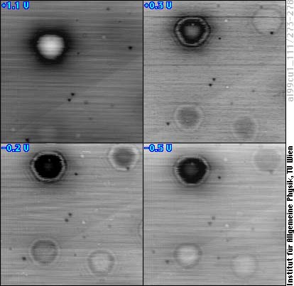
Each frame shows approximately the same area (30 nm x 30 nm). You can clearly see how the interference patterns caused by the bubbles change brightness with voltage, and, hence, energy. Exploiting the change of the image with different voltages, we can determine the depth of the bubbles. We find that there are at least approx. 6 layers of Al atoms separating the bubble from the surface, but there are also many deeper bubbles. As expected, deeper bubbles appear weaker in the STM images.
For further information
- A textbook on surface physics, including surface states, the Wulff construction etc.
Andrew Zangwill
Physics at surfaces
Cambridge University Press 1988.- Scattering of Cu(111) surface states by Pb
C. Nagl, O. Haller, E. Platzgummer, M. Schmid and P. Varga
Submonolayer growth of Pb on Cu(111): Surface alloying and de-alloying
Surf. Sci. 321 (1994) 237-248. Full text*- Scattering of surface states by subsurface impurities (theoretical)
S. Crampin
Surface states a probes of buried impurities
J. Phys. Condens. Matter 6 (1994) L613-L618.- Surface states of Fe and FeSi/Fe (d-orbitals)
A. Biedermann, O. Genser, W. Hebenstreit, M. Schmid, J. Redinger, R. Podloucky, and P. Varga
Scanning tunneling spectroscopy of one-dimensional surface states on a metal surface
Phys. Rev. Lett. 76 (1996) 4179-4182. Full text- Bulk electron scattering by Ar bubbles
M. Schmid, W. Hebenstreit, P. Varga, S. Crampin
Quantum wells and electron interference phenomena in Al due to subsurface noble gas bubbles
Phys. Rev. Lett. 76 (1996) 2298-2301. Full textM. Schmid, S. Crampin, P. Varga
STM and STS of bulk electron scattering by subsurface objects
J. Electron Spectrosc. Relat. Phen. 109 (2000) 71-84. Full text*
* Please note: access to full text (PDF files) of some articles is restricted due to copyright reasons.
If you find for errors on this page, let me know:
Michael Schmid, IAP/TU Wien ([email address: lastname @ this server · enable javascript to see it]).
