The Scanning Tunneling Microscope
What it is and how it works …
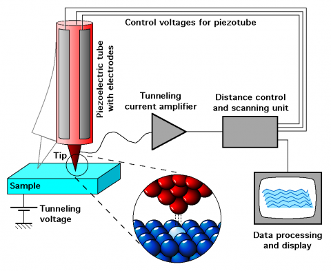
Scanning tunneling microscopy is a technique developed in the eighties and provides images of solid surfaces with unprecedented resolution. The operation of a scanning tunneling microscope (STM) is based on the so-called tunneling current, which starts to flow when a sharp tip approaches a conducting surface at a distance of approximately one nanometer. The tip is mounted on a piezoelectric tube, which allows tiny movements by applying a voltage at its electrodes. Thereby, the electronics of the STM system control the tip position in such a way that the tunneling current and, hence, the tip-surface distance is kept constant, while at the same time scanning a small area of the sample surface. This movement is recorded and can be displayed as an image of the surface topography. Under ideal circumstances, the individual atoms of a surface can be resolved and displayed.
This explanation is illustrated by an animated sequence.

Copyright notice: See below
It should be noted, however, that STM images not only display the geometric structure of the surface, but also depend on the electronic density of states of the sample, as well as on special tip-sample interaction mechanisms which are not fully understood yet.
Although the STM itself does not need vacuum to operate (it works in air as well as under liquids), ultrahigh vacuum is required to avoid contamination of the samples from the surrounding medium.
A problem in investigating metal surfaces is the fact that these surfaces appear very flat to an STM, i.e., the apparent height of individual atoms (corrugation) is 1/100 to 1/10 of an atomic diameter. Therefore, for resolving individual atoms the distance between the tip and the sample must be kept constant within 1/100 of an atomic diameter or better (approx. 0.002 nm). This demands not only very high rigidity of the STM itself, but the STM must be also efficiently decoupled from environmental vibrations.
STM images are usually displayed as greyscale images with protrusions shown white and depressions black. Many images in our STM Gallery are raw data (except for background subtraction), which may be slightly smoothed by interpolation to the image size used for display; in a few cases image processing has been used for contrast enhancement to display both the atomic corrugation and a larger height range such as different layers of atoms.
The STMs at IAP/TU Wien
 Most STM images in this Gallery were taken with the room-temperature STM; a few also with the low-temperature STM in the Surface Physics Group. Both instruments operate in ultrahigh vacuum; a prerequisite for studying clean metal surfaces.
For further information
- The inventors of the STM
Gerd Binnig and Heinrich Rohrer, have been awarded the Nobel Prize in Physics 1986 (together with Ernst Ruska, who was honored for the design of the first conventional electron microscope). See the press release of the Nobel Foundation.
- Introductionary texts
- G. Binnig, H. Rohrer, Scientific American, Vol. 253, Aug. 1985, pp. 40-46.
- C. F. Quate, Physics Today, Vol. 39, Aug. 1986, pp. 26-33.
- G. Binnig, H. Rohrer, Reviews of Modern Physics, Vol. 71, No. 2 (1999), pp. S324-S330.
- H. Fuchs, Physikalische Blätter, Vol. 45, Nr. 4 (1989), pp. 105-115 (in German).
- Review articles
- G. Binnig, H. Rohrer, IBM J. Res. Develop. 30 (1986), pp. 355-369.
- J.E. Griffith, G. E. Kochanski, Annu. Rev. Mater. Sci. 20 (1990), pp. 219-244.
- T. Sakurai et al., Progr. Surf. Sci. 33 (1990), pp. 3-89.
- L.E.C. van de Leemput, H. van Kempen, Rep. Prog. Phys. 55 (1992), pp. 1165-1240.
- Overview articles dealing with instrumental aspects of STM
- D. W. Pohl, IBM J. Res. Develop. 30 (1986), pp. 417-427.
- Y. Kuk, P.J. Silverman, Rev. Sci. Instrum. 60 (1989), pp. 165-180.
- The proceedings of the first STM conference 1985
…were published in IBM J. Res. Develop. Vol. 30, Nos. 4 and 5 (1986). Many articles therein are still interesting today.
The schematic drawing of the STM and the text of this page may be used under Creative Commons Attribution ShareAlike 2.0 Austria License (provided that the name of the author is given, e.g. “Figure: Michael Schmid, TU Wien” in the figure caption when the figure is used). The figure is also available at Wikimedia Commons.
This page, including all the typos, was created by Michael Schmid ([email address: lastname @ this server · enable javascript to see it]).