Growth of Copper in Lead
Unexpected, but explicable
Lead and copper are immiscible metals due to the large difference in atomic size - Pb atoms are 37% larger than Cu atoms. Since the surface energy (the energy required to “cut through” the bonds of a crystal to create a surface) of Pb is significantly smaller than that of Cu, standard growth theory would expect that Cu islands should grow on the Pb substrate.
Pb atoms are very mobile (that is why lead is so soft and can be melted so easily), so all that we show here happens already at room temperature.
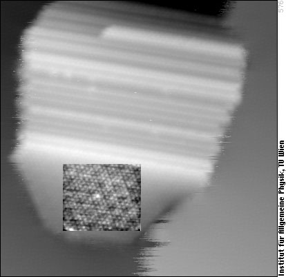
Now let us have a look at some Cu deposited on Pb(111):
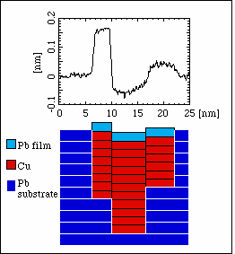
We see a pear-shaped island, but we note that the lattice constant of the hexagonal atomic grid is that of Pb, also on the island. If one looks more carefully, one can see a moiré pattern on the island, which is exactly that of one monolayer Pb on Cu(111). Since such moiré patterns are very sensitive even to subtle changes in the structure, it is clear that we see one Pb layer on a Cu island.
Whereas the Pb film (and, hence, the subsurface Cu island) has the same orientation as the Pb substrate in the previous STM image, it may be also rotated by 30°. This can be seen in the following image:
Here the island reaches somewhat further out of the surface, but an analysis of the linescan again shows us that the Cu grows into the surface, not on top of it.
So what is the reason for that peculiar growth mode? First of all, the surface energy of Pb (0.5 J/m2) is much lower than that of Cu (1.96 J/m2). In other words, the energetic cost of creating a Cu surface is much higher than that of creating a Pb surface. Since nature tries to minimize energy, it is clear that a Cu island covered by Pb is favorable.
The reason why the Cu islands do not grow on top of, but rather into the substrate is similar: An island situated on Pb has also a surface at its sides, which costs surface energy (only the one of Pb, if it is covered with it). But the energy can be further reduced by trading in this surface energy for the even lower interface energy at the sides of a Cu island embedded in Pb.
So let us look at this drawing to see what happens:

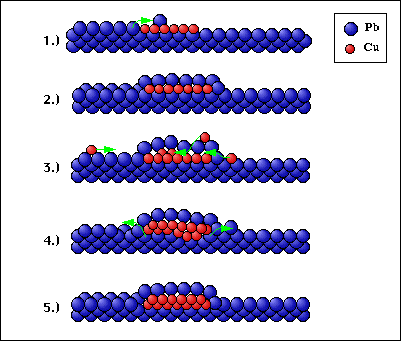
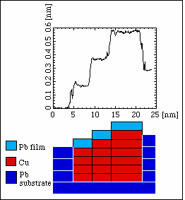
As soon as some Cu atoms assemble on the Pb surface (1), the mobile Pb atoms cover the Cu (2). Additional Cu atoms are wandering about until they find one of these subsurface Cu islands where they are readily incorporated (3). Since the island tends to minimize its surface (see above), it tries to sink into the Pb. This can be done by diffusion of Pb atoms from below the island to the surface (4). This must not necessarily lead to an island well aligned with the surface, as shown in (5) or in the previous STM images. It can also happen that Pb diffuses up faster on one side of the Cu island than on the other, in this case the island becomes tilted.
And that is what such a tilted island looks like in the STM:

For further information
- C. Nagl, E. Platzgummer, M. Schmid, P. Varga, S. Speller and W. Heiland
Direct Observation of a New Growth Mode: Subsurface Island Growth of Cu on Pb(111)
Phys. Rev. Lett. 75 (1995) 2976-2979. Full text
Please note that the atomically resolved STM images have been reproduced incorrectly in the printed article (i.e., the paper version of Phys. Rev. Lett.). The correct versions of these figures are shown above (fig. 2 and fig. 3), in the PDF file and in PRL 76 (1996) 3240 (E).
- C. Nagl, E. Platzgummer, M. Schmid, P. Varga, S. Speller and W. Heiland
Subsurface islands and superstructures of Cu on Pb(111)
Surf. Sci. 352-354 (1996) 540-545.
- More on the moiré pattern of Pb/Cu/Pb(111):
C. Nagl, M. Schmid, and P. Varga
Inverse corrugation and corrugation enhancement of Pb superstructures on Cu(111) and (110)
Surf. Sci 369 (1996) 159-168. Full text*
* Please note: access to full text (PDF files) of some articles is restricted due to copyright reasons.
If you like our STM Gallery, tell it your colleagues. If you find errors, please send an e-mail to Michael Schmid, IAP/TU Wien ([email address: lastname @ this server · enable javascript to see it]).


