Growth of Lead on Copper
An atomic maze and other surprises
Lead deposited on copper was one of the first systems of metal-on-metal growth studied by surface scientists. Nevertheless, many structures had to wait for the application of the scanning tunneling microscope to be understood.
The crystal structure of both lead and copper is face centered cubic (fcc), but due to their difference in atomic size (Pb atoms are 37% larger than Cu atoms), these two materials are strictly immiscible in the bulk. Nevertheless, the STM has shown us that Pb and Cu can easily intermix in the surface layer.
Pb on Cu(111)
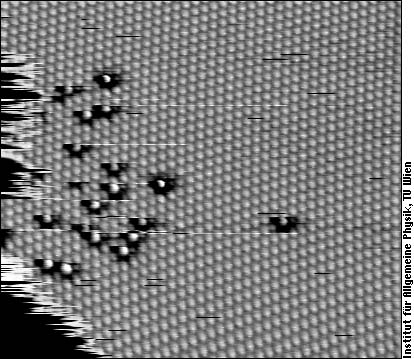
On (111)-oriented Cu surfaces, it all starts with a surface alloy, i.e., some Cu atoms are replaced by Pb. It is quite tricky to get atomic resolution on the Cu surface and not disturb the structure too much, since one has to approach the STM tip to a rather close distance, where it interacts with the Pb atoms (those with a dark “halo”). The tip-sample interaction also causes movement of atoms at the monatomic step in the left part of the image and makes it appear frizzy.
With increasing Pb deposition and gentle heating (to facilitate the exchange between Pb and Cu atoms in the surface), the surface alloy contains more and more Pb atoms up to a maximum density, where approx. 22 % of the Cu atoms are replaced by Pb. In the following STM image of this disordered surface alloy, only the Pb atoms are visible, not the Cu's. The Pb atoms are still surrounded by 6 (invisible) Cu neighbours each, but usually there are 2 or 3 Pb (and 4 or 3 Cu) next-nearest neighbours to a Pb atom.
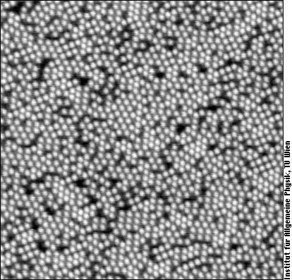
One puzzling feature of this structure is that it remains disordered even if we “melt” it and then cool it down very slowly (over many hours). Most metal-on-metal structures known so far would “crystallize” in a well-ordered pattern.
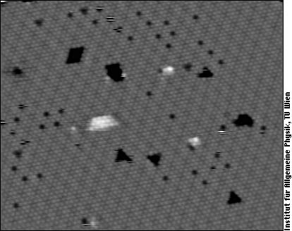
At higher coverages of Pb, a full monolayer of Pb atoms forms, which may exhibit some defects like vacancies, i.e., missing Pb atoms (black spots) and Pb atoms on top of Pb embedded in the second layer (bright).
Due to the difference in atomic size of Pb and Cu, 3×3 Pb atoms cover 4×4 Cu atoms. This structure is therefore called a (4×4) superstructure. You can also consider it a moiré pattern formed when two grids with different lattice constants are superimposed.
Pb on Cu(100)
On (100)-oriented copper, we also find a disordered surface alloy at low coverages of Pb. When we deposit 3 Pb atoms per 8 Cu surface atoms (coverage 3/8 = 0.375), a well-ordered structure appears:
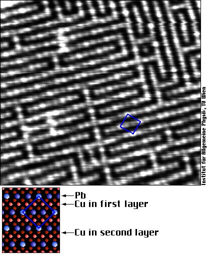
As the structure model shows, the bright “walls” of the maze are rows of Pb atoms (again 3 Pb atoms on 4 Cu atoms), and there are rows of Cu atoms between them (dark and unresolved in STM images).
Pb on Cu(110)
At low coverages, Pb also forms disordered surface alloys at (110)-oriented Cu surfaces, but a large variety of superstructures are found at coverages between 0.5 and 0.8. Let us just have a look at the one with the highest Pb coverage:
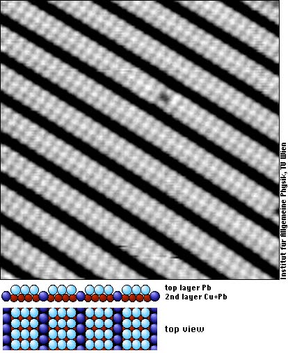
Although we see triple rows of Pb atoms in the STM image, and nothing in the dark grooves (the STM tip is not sharp enough to probe the grooves), we know that there must be Pb rows also in the grooves (we know the exact amount of Pb deposited). The structure model shows that these Pb atoms replace each fifth Cu atom in the layer below. This means that also this structure is a kind of surface alloy, where Pb atoms replace surface atoms of Cu.
At room temperature, there is no pure overlayer structure of Pb/Cu(110) such as the one on Cu(111) shown above, but one can only have various surface alloy phases with Pb and Cu mixed up in the same atomic layer. And this, although Pb and Cu are immiscible in the bulk!
For further information
Unless noted otherwise, the structures shown here form already at room temperature. The defects on the close-packed Pb/Cu(111) layer are probably due to bombardment of the sample with a few high-energy (800 eV) Pb ions created in the evaporator.
- Pb/Cu(111)
C. Nagl, O. Haller, E. Platzgummer, M. Schmid and P. Varga
Submonolayer growth of Pb on Cu(111): Surface alloying and de-alloying
Surf. Sci. 321 (1994) 237-248. Full text*- Pb/Cu(100)
C. Nagl, E. Platzgummer, O. Haller, M. Schmid and P. Varga
Surface alloying and superstructures of Pb on Cu(100)
Surf. Sci. 331-333 (1995) 831-837. Full text*- Pb/Cu(110)
C. Nagl, M. Pinczolits, M. Schmid and P. Varga
p(nx1) superstructures of Pb on Cu(110)
Phys. Rev. B 52 (1995) 16796-16802. Full text- More ...
More (i.e., simulation calculations) about the moiré pattern of Pb/Cu(111) and the detailed structure of Pb/Cu(110) can be found in:
C. Nagl, M. Schmid, and P. Varga
Inverse corrugation and corrugation enhancement of Pb superstructures on Cu(111) and (110)
Surf. Sci 369 (1996) 159-168. Full text*
* Please note: access to full text (PDF files) of some articles is restricted due to copyright reasons.
Whom you should blame for possible errors on this page:
Michael Schmid, IAP/TU Wien ([email address: lastname @ this server · enable javascript to see it]).


